Q1: What are the basic amplifier configurations? $\frac {g_mr_\pi R_E}{1+(\frac{R'_L}{r_o})(1+\frac{R_E}{r_\pi})}$
A1: There are 8 basic amplifier configurations: 4 basic BJT amplifier configurations and 4 basic MOS amplifier configurations. Note that that taking the limit as $r_\pi \to \infty$ of the BJT equations produces the MOS equations.
 |
| Common Base:
$A_v=g_m(r_o || R'_L)$
$R_i=r_\pi || \frac {r_o+R'_L}{1+g_mr_o}$
|
 |
| Common Gate:
$A_v=g_m(r_o || R'_L)$
$R_i= \frac {r_o+R'_L}{1+g_mr_o}$ |
 |
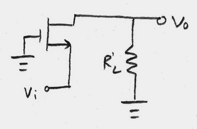
Common Source:
$A_v=-g_m(r_o || R'_L)$
$R_i=\infty$
|
 |
| Common Emitter: $A_v=-g_m(r_o || R'_L)$ $R_i=r_\pi$ |
 |
| Common Emitter with $R_E$:
$A_v=-\frac{g_mR'_L}{1+g_mR_E+(R'_L/r_o)(1+R_E/r_\pi)}$
$R_i=r_\pi + \frac {g_mr_\pi R_E}{1+(R'_L/r_o)(1+R_E/r_\pi)}$
|
 |
Common Source with $R_S$:
$A_v=-\frac{g_mR'_L}{1+g_mR_E+(R'_L/r_o)}$
$R_i=\infty$
|
 |
| Common Collector/Emitter Follower:
$A_v=\frac{g_m(r_o || R'_L)}{1+g_m(r_o || R'_L)}$
$R_i=r_\pi + \beta (r_o || R'_L)$
|
 |
| Common Drain/Source Follower:
$A_v=\frac{g_m(r_o || R'_L)}{1+g_m(r_o || R'_L)}$
$R_i=\infty$
|


